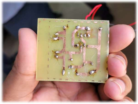
PCB fabrication is the process or procedure that transforms a circuit board design into a physical structure based upon the specifications provided in the design package. This physical manifestation is achieved through the following techniques:
• Imaging desired layout on copper clad laminates
• Etching or removing excess copper from inner layers to reveal traces and pads • Creating the PCB layer stack up by laminating (heating and pressing) board materials at high temperatures
• Drilling holes for mounting holes, through hole pins and vias
• Etching or removing excess copper from the surface layer(s) to reveal traces and pads • Plating pin holes and via holes
• Adding protective coating to surface or solder masking
• Silkscreen printing reference and polarity indicators, logos, or other markings on the surface
• Optionally, a finish may be added to copper areas of surface